Background
The KENBAK-1 was developed by John Blankenbaker (and was named after him) in the early 1970s as a teaching tool. Its design guidelines were that it had to be low-cost, educational and able to satisfy the users with simple programs. It could be a serial computer, hence a slow one, which would have reduced the costs and yet meet the such requirements. It would have to handle as many programming concepts as possible. Due to its small size, its native language would have been the machine language. Above all, it had to be a stored-program computer (Von Neumann machine). The aim was to design a simple computer.
Designed before microprocessors were available, its logic consisted of 132 standard TTL integrated circuits mounted on a single PCB. The serial memory was implemented using 2 MOS shift registers of 1024 bits each, for a total of 2048 bits. Input was accomplished via switches and output was displayed via LEDs. Although the computer had a clock of 1 MHz, it processed only a few hundred instructions per second, because it had a serial architecture, so it processed only one bit at a time.
Critical issues
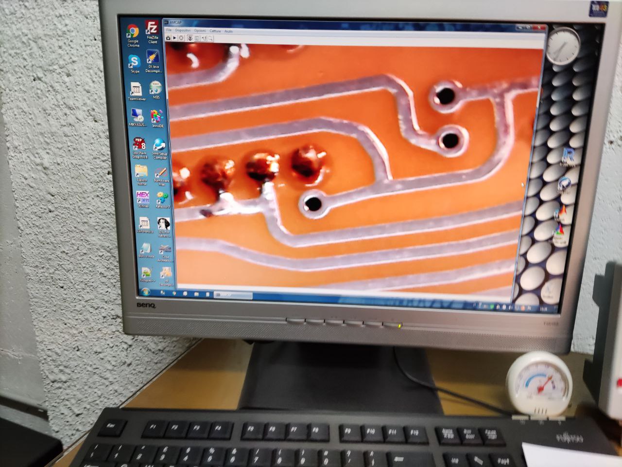
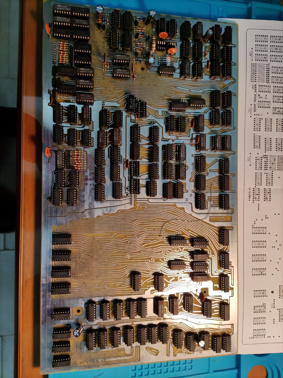
• The PCB has to be made starting from photos: high-resolution ones are available but with components mounted, those without components are low-resolution ones. We will try to overlap them to get the complete traces.
• There is one component (1404a) quite rare, and 4-5 others of medium rarity.
• Case dimensions have to be deduced from indirect information, such as photos and proportions compared to other objects whose real dimensions are known.
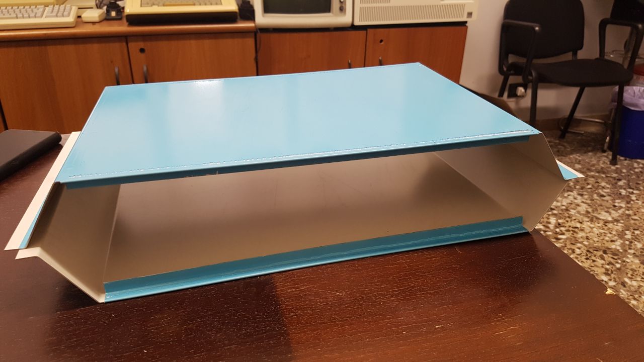
• The need to reproduce the mechanics.
Realization
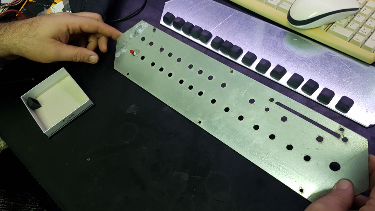
The realization of the printed circuit board was made possible thanks to the patient work carried out by Stefano Ferilli (printed circuit design) and Gianfranco Mazzarello (production of the gerber file essential for the board production). Subsequently, the team composed of the manager, Michele Perniola, and Stefano himself, moved on to the realization of the prototype. The realization of the front panel was made possible thanks to the electrical components and the metal hexagon made available by Stefano. The realization of the case was made possible thanks to the commitment and competence of Vito Fariello.
Here are some photos that show the work done.
December 30, 2021 update
January 15, 2022 update
January 24, 2022 update
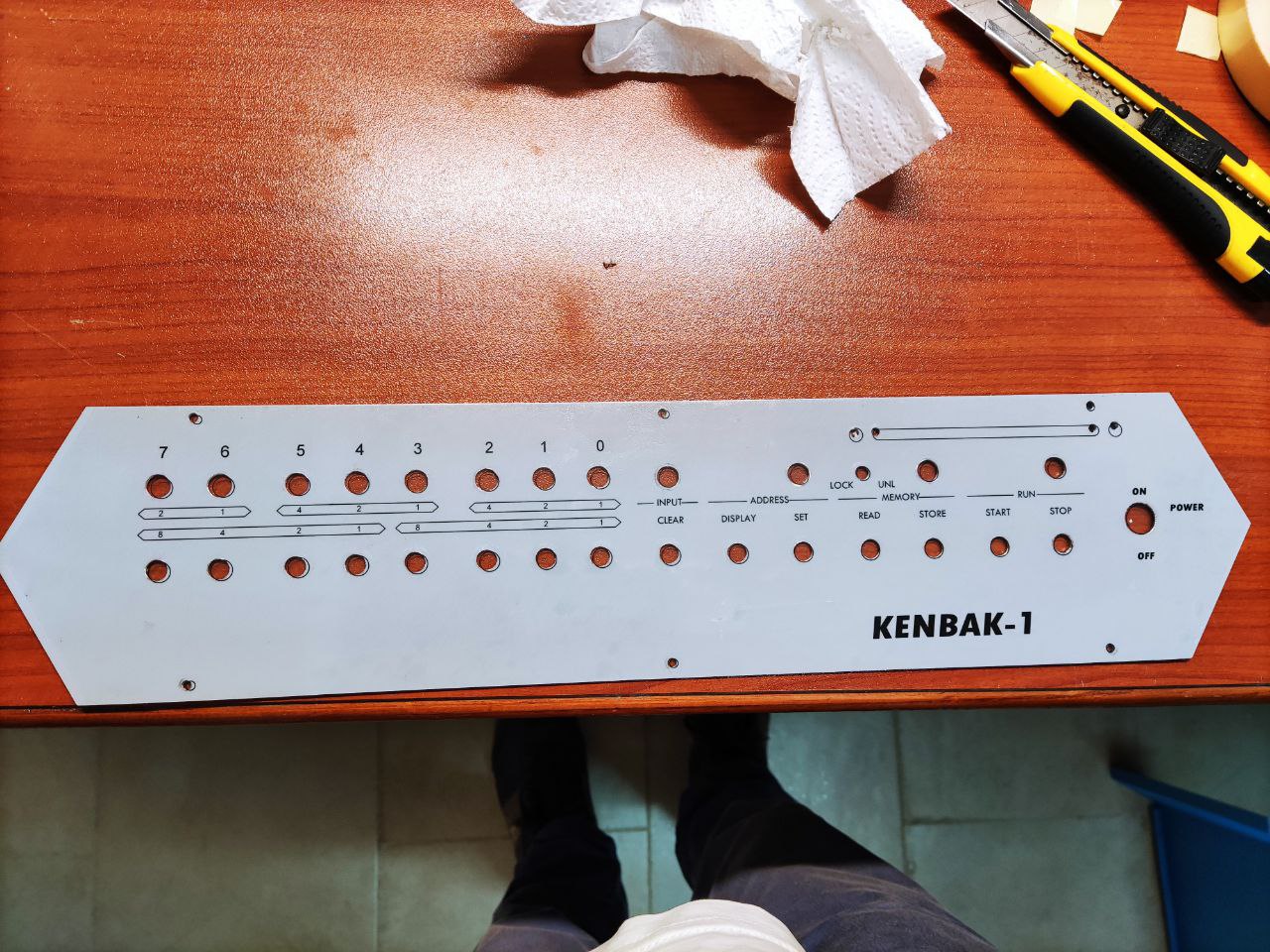
Paper labels were attached with transparent Magic tape. It is a temporary solution we can remove without causing any damage to the panel.
The key caps made by Vito Fariello were fitted.
January 31, 2022 update
Front panel wiring.
April 13, 2022 update
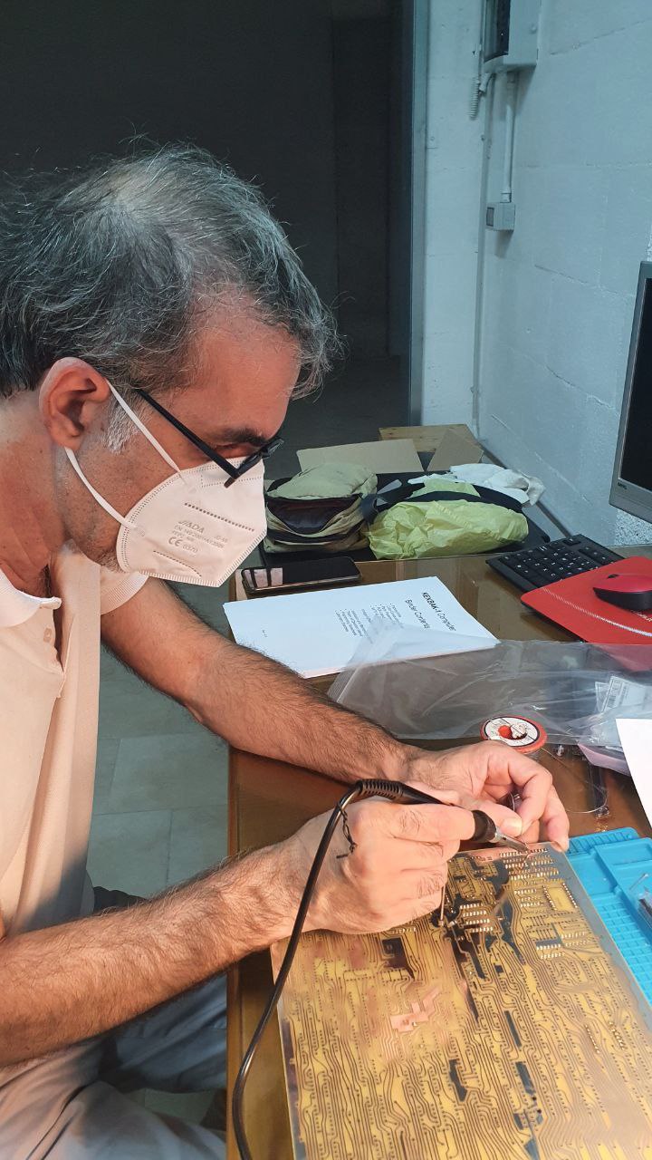
Short circuit hunt on the printed circuit board.
… there is no short circuit. Unfortunately, SN74LS54 ICs have been supplied instead of SN7454. This is one of the few cases where the ’74LS’ series IC is not a valid substitute for the corresponding ’74’ series, as they have a completely different pinout 😖. We had to order correct ICs: they should arrive in the next few days.
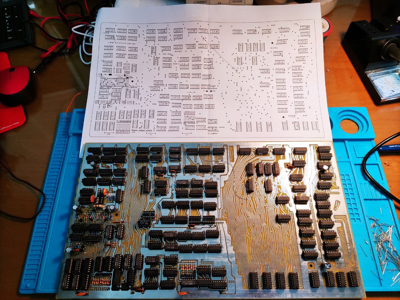
Manual and diagrams ready for debugging
April 20, 2022 update
“Memories” (shift registers 1024 bit SY1404A) have been installed.
An error has been identified on the printed circuit board under the IC 104. The socket has been removed, the track has been cut and a new jumper has been installed (next to the one previously made to replace the missing track).
April 24, 2022 update
Unfortunately, the very difficult acquisition of the printed circuit design “didn’t come out well”, especially on the component side, where the only good photo available was…with the components soldered.
About 16 errors were identified considering both missing and incorrectly connected tracks.
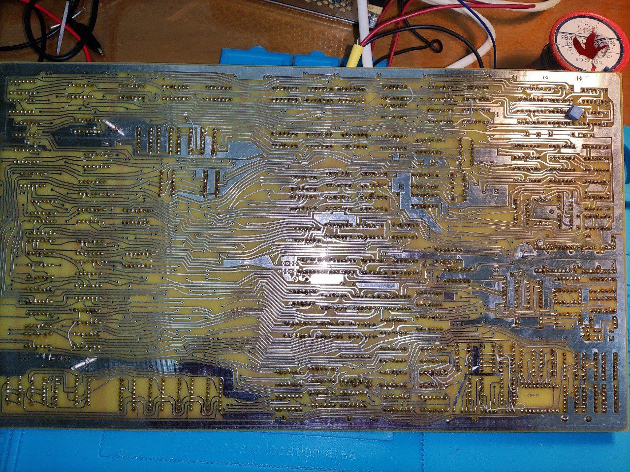
The tracks have been temporarily “fixed”. Some fixes were done by unsoldering sockets to cut bad tracks underneath them.
The behavior of the lights/buttons now feels “more natural”.
The next step will be the check of the test patterns reported in the Kenbak manual.
May 26, 2022 update
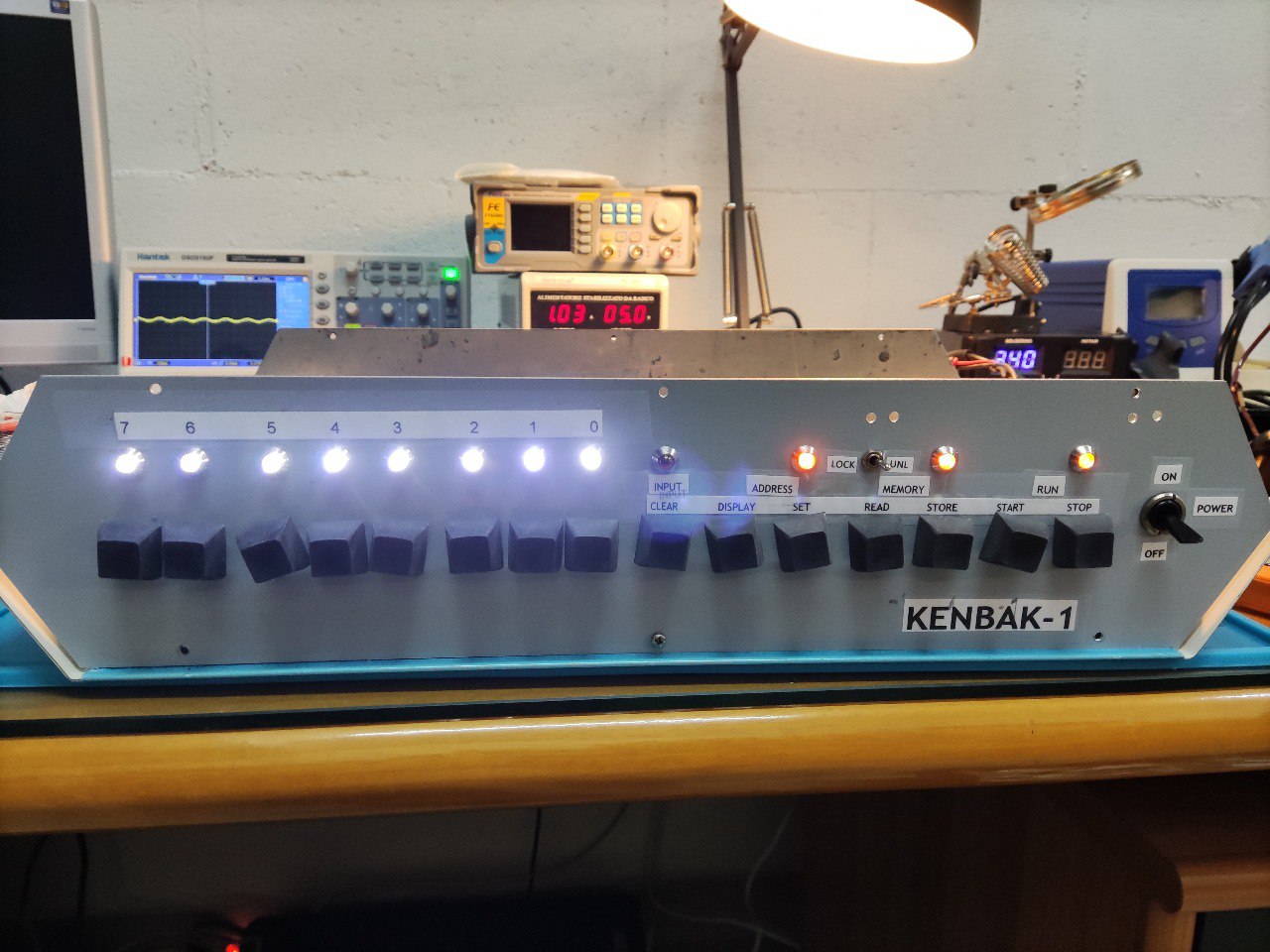
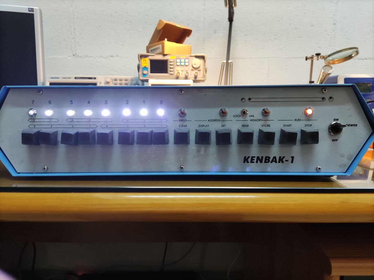
The Kenbak-1 prototype is finally functional. It has been tested with an appropriate program included in the manual, which results in the scrolling of the indicator lights.
June 2, 2022 update
We move on to painting the case.
Stages of assembly.
The adhesive printed panel arrived.
Final stages of the assembly…
Video of the test of the completed prototype behaviour.
Photo of the assembled prototype.
I have just found this article, and have found it fascinating. You have untook a monumental feat. I think only a handful of people have managed to recreate the Kenbak-1, and with the many problems (errors in the printed circuit board, problems with transistor configuration, etc) I was surprised to see you got it working!!! I’m very impressed.
Would it be possible to link to your site, and possibly even use some of your photos (with proper attribution and link back to your site) at our kenbak.com web site? Your success in recreating the Kenbak-1 from scratch would fit in well with our attempt to chronicle the several people who have made Kenbak-1 computers from scratch.
Hello there.
Yes, for sure you can link our site and use every photo you need. Thanks for your kindness.
The Staff